
")
In the intricate world of printed circuit board (PCB) design, technological advancements constantly reshape the landscape. One such innovation that has significantly impacted PCB design is the advent of blind vias. This article delves into the definition, importance, and wide-ranging applications of blind vias in modern PCB design.
Understanding Blind Vias
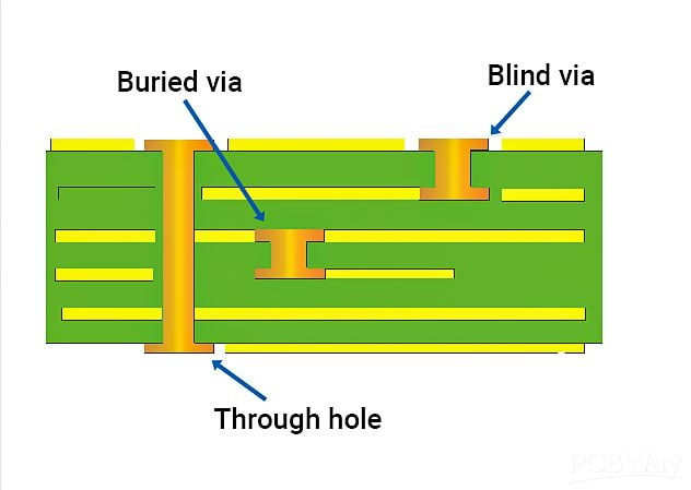
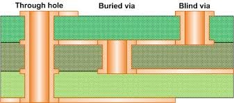
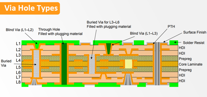
Blind vias are microscopic holes drilled into PCBs that connect an outer layer to one or more inner layers, without penetrating the entire board. Unlike through-hole vias that traverse the entire board, blind vias only extend partway, terminating at an inner layer. This unique construction enables complex multilayer PCB designs with enhanced functionality and reduced space requirements.
Some Fundamentals and History of Origin—Blind Vias
Fundamentals of Blind Vias
Blind vias are a type of via (vertical interconnect access) in printed circuit boards (PCBs) that connect an outer layer to one or more inner layers without passing through the entire board. Here are the key fundamentals of blind vias:
- Partial Depth Drilling: Blind vias are drilled only partway into the PCB, stopping at a designated inner layer. This contrasts with through-hole vias, which extend from one outer layer to the other, traversing all the board layers.
- Microvia Technology: Often created using advanced microvia technology, blind vias typically have smaller diameters than traditional through-hole vias. This allows for more compact and densely packed PCB designs.
- Electroplating and Filling: After drilling, blind vias are usually electroplated with copper to create a conductive path between layers. In some cases, they are filled with conductive or non-conductive material to enhance structural integrity and prevent solder migration.
- Design and Layout Considerations: Incorporating blind vias into PCB design requires careful planning. Designers must ensure proper alignment with the corresponding inner layers and consider factors like signal integrity, thermal management, and mechanical stability.
History of Blind Vias
The development and adoption of blind vias have been driven by the ongoing miniaturization and complexity of electronic devices. Here is a brief history of their origin and evolution:
- Early PCB Design: In the early days of PCB design, single-sided and double-sided boards with through-hole vias were the norm. These early designs were sufficient for simple electronic circuits with relatively few components.
- Rise of Multilayer PCBs: As electronic devices became more complex, the demand for multilayer PCBs grew. The introduction of multilayer PCBs in the 1960s allowed for more intricate and compact designs, but through-hole vias were still the primary means of interconnecting layers.
- Emergence of HDI Technology: The 1980s and 1990s saw the rise of high-density interconnect (HDI) technology. HDI enabled the creation of PCBs with finer traces, smaller vias, and higher layer counts. It was during this period that blind vias began to gain prominence as a way to optimize space and improve signal integrity in HDI designs.
- Advancements in Drilling Techniques: The development of laser drilling and other precision drilling techniques in the late 20th and early 21st centuries further advanced the use of blind vias. These techniques allowed for the creation of microvias, significantly reducing via size and enabling more compact and high-performance PCB designs.
- Widespread Adoption in Modern Electronics: Today, blind vias are a standard feature in many advanced electronic devices, from smartphones and tablets to aerospace and medical equipment. Their ability to enhance design flexibility, improve signal integrity, and optimize thermal management has made them indispensable in the ever-evolving landscape of PCB design.
Importance of Blind Vias
- Space Optimization: By allowing connections between layers without going through the entire board, blind vias free up valuable space on PCBs. This is especially crucial in miniaturized electronic devices where every millimeter counts.
- Improved Signal Integrity: Blind vias minimize signal interference and impedance discontinuities, leading to improved signal integrity and reduced electromagnetic interference (EMI). This is vital for high-speed digital circuits and RF applications.
- Enhanced Thermal Management: In PCBs with blind vias, heat dissipation is more efficient. By strategically placing blind vias near heat-generating components, designers can enhance thermal management and prolong component lifespan.
- Design Flexibility: Blind vias offer greater design flexibility by enabling the creation of complex multilayer PCBs with varied routing options. This flexibility fosters innovation and allows for more sophisticated electronic designs.
Applications of Blind Vias
- Mobile Devices: Smartphones, tablets, and wearables benefit from blind vias due to their compact size and the need for intricate multilayer PCBs to accommodate various functionalities.
- High-Speed PCBs: Blind vias are crucial in high-speed PCBs used in data centers, telecommunications equipment, and high-performance computing systems. They facilitate efficient signal transmission and reduce signal degradation.
- Aerospace and Defense: In aerospace and defense electronics, where reliability and miniaturization are paramount, blind vias play a vital role in ensuring robust and compact PCB designs for avionics, satellites, and military equipment.
- Medical Devices: Medical electronics often require compact and reliable PCBs. Blind vias enable the creation of intricate medical devices such as implantable devices, diagnostic equipment, and monitoring systems.
- Automotive Electronics: Blind vias are used extensively in automotive electronics for control units, infotainment systems, and advanced driver-assistance systems (ADAS), where space constraints and reliability are critical factors.
The four types of blind vias are:
In PCB design, blind vias come in several types, each serving specific purposes based on their construction and application. Here are the four main types of blind vias and a discussion of each:
1. Sequential Lamination Blind Vias
Description: Sequential lamination blind vias are created by laminating and drilling the PCB in multiple stages. Each stage involves drilling vias, plating, and then adding another layer before repeating the process.
Discussion: This method allows for more complex and densely packed PCB designs. By building the board layer by layer, designers can achieve greater interconnect density and improved electrical performance. Sequential lamination is particularly useful for high-density interconnect (HDI) boards, where space optimization and signal integrity are critical. However, the process is more time-consuming and costly compared to simpler via types.
2. Controlled Depth Blind Vias
Description: Controlled depth blind vias are drilled to a precise depth, stopping at a specific inner layer without penetrating through the entire PCB. This precision is typically achieved using laser drilling or mechanical drilling with depth control.
3. Stacked Blind Vias
Description: Stacked blind vias are created by stacking multiple blind vias on top of each other across different layers of the PCB. Each via is drilled, plated, and filled before the next via is added on top in a subsequent layer.
Discussion: Stacked blind vias allow for vertical interconnections through multiple layers of the PCB, enabling more complex routing and higher component density. This technique is beneficial in applications where space is limited and multi-layer interconnects are necessary. The stacking process, however, requires precise alignment and can increase manufacturing complexity and cost. It is commonly used in advanced HDI boards and high-performance applications like smartphones and tablets.
4. Staggered Blind Vias
Description: Staggered blind vias are offset in position across different layers, rather than being aligned vertically. Each via connects specific layers but does not align with vias in adjacent layers.
Discussion: Staggered blind vias provide flexibility in routing and can help distribute thermal and mechanical stresses more evenly across the PCB. This type of via is advantageous in designs where routing constraints and thermal management are significant concerns. By staggering the vias, designers can optimize the layout to avoid congestion and improve overall board reliability. This method is particularly useful in complex multilayer designs where space optimization and heat dissipation are critical.
The Electrical Advantages of Blind Vias
Blind vias offer several electrical advantages in printed circuit board (PCB) design, making them a crucial element in modern electronic devices. Here are some key electrical benefits of using blind vias:
Improved Signal Integrity
Blind vias enhance signal integrity by minimizing the length of the conductive path between layers. Shorter paths reduce signal distortion, reflections, and loss, which is especially important in high-speed and high-frequency applications. This results in more reliable and accurate signal transmission, which is critical for maintaining the performance of advanced electronic systems.
Reduced Electromagnetic Interference (EMI)
By limiting the via to specific layers, blind vias help reduce electromagnetic interference. They prevent signals from spreading across multiple layers, thereby minimizing crosstalk and EMI. This is particularly beneficial in densely packed PCBs where multiple high-frequency signals coexist, ensuring that each signal maintains its integrity without interference from adjacent signals.
Optimized Layer Utilization
Blind vias allow for more efficient use of the available layers in a PCB. By connecting only the necessary layers, designers can allocate more space for signal routing on the inner layers. This optimization leads to improved overall board performance and the ability to handle more complex and higher-density designs without compromising electrical performance.
Enhanced Power Distribution
In multilayer PCBs, power distribution networks can be designed more effectively using blind vias. They allow for direct connections between power planes and specific layers, reducing the impedance and resistance in the power distribution path. This results in more stable and efficient power delivery to components, enhancing the overall performance and reliability of the PCB.
Lower Parasitic Capacitance and Inductance
Blind vias reduce parasitic capacitance and inductance, which can negatively impact signal integrity. Traditional through-hole vias introduce additional capacitance and inductance due to their longer conductive paths. By shortening the path, blind vias minimize these parasitic elements, leading to better signal quality and reduced noise in high-speed circuits.
Minimized Signal Delays
Blind vias help minimize signal propagation delays by shortening the conductive path between layers. This is particularly important in high-speed digital circuits where timing is critical. Reduced delays lead to faster signal transmission and improved synchronization between different parts of the circuit, enhancing overall performance.
Improved Grounding and Shielding
By providing direct connections between ground planes and specific layers, blind vias enhance grounding and shielding within the PCB. This improves the overall electromagnetic compatibility (EMC) of the board, reducing the risk of signal interference and ensuring better protection against external electromagnetic disturbances.
The Shortcomings of Blind Vias

While blind vias offer significant advantages in PCB design, they also come with certain shortcomings that designers and manufacturers need to consider. Here are some key challenges and limitations associated with blind vias:
Increased Manufacturing Complexity
Blind vias require more sophisticated drilling techniques, such as laser drilling or controlled depth mechanical drilling. These methods demand high precision and accuracy, making the manufacturing process more complex. This complexity can lead to longer production times and higher chances of defects if not properly managed.
Higher Costs
The increased complexity of manufacturing blind vias translates into higher production costs. The need for advanced equipment, additional process steps, and stringent quality control measures all contribute to the overall cost. For designs with a high number of blind vias, these costs can become significant, impacting the economic feasibility of the project.
Limited Depth
Blind vias have a depth limitation, as they can only connect a few layers within the PCB. This restricts their use in extremely thick or highly multilayered boards. For applications requiring interconnections across many layers, other types of vias, such as buried or through-hole vias, might be more appropriate.
Potential Reliability Issues
If not properly designed or manufactured, blind vias can introduce reliability issues. Factors such as misalignment, insufficient plating, or voids in the via can lead to electrical failures or reduced mechanical strength. Ensuring high reliability requires meticulous design and stringent manufacturing controls, which can be challenging to maintain consistently.
Design and Layout Constraints
Incorporating blind vias into a PCB design requires careful planning and can impose constraints on the layout. Designers must consider factors like the placement of components, signal routing paths, and thermal management strategies. These constraints can limit design flexibility and may necessitate compromises in other areas of the PCB design.
Thermal Stress
Blind vias can be more susceptible to thermal stress compared to through-hole vias. The difference in thermal expansion coefficients between the via and the surrounding material can cause stress, especially during thermal cycling. This can lead to via fatigue, cracking, or delamination over time, particularly in high-temperature environments.
Inspection and Testing Challenges
Inspecting and testing blind vias is more challenging than for through-hole vias. Traditional visual inspection methods are often insufficient, requiring advanced techniques like X-ray inspection to detect potential issues. This adds to the overall complexity and cost of quality assurance processes.
Limited Application in Some PCB Technologies
While blind vias are beneficial in high-density interconnect (HDI) and advanced PCB technologies, they might not be suitable for all types of PCBs. In simpler, lower-cost, or lower-layer-count designs, the benefits of blind vias may not justify the additional complexity and expense, making them less practical for such applications.
Advantages of using blind vias
Blind vias offer numerous benefits that can significantly enhance the design and performance of printed circuit boards (PCBs). Here are the key advantages of using blind vias:
- Space Optimization
Blind vias help save valuable real estate on the PCB by connecting layers without passing through the entire board. This allows designers to create more compact and densely packed PCBs, which is particularly important in miniaturized electronic devices like smartphones, tablets, and wearable technology.
- Improved Signal Integrity
By shortening the conductive path between layers, blind vias reduce signal distortion, reflections, and loss. This leads to better signal integrity, which is crucial for high-speed and high-frequency applications where maintaining clean and accurate signal transmission is essential.
- Reduced Electromagnetic Interference (EMI)
Blind vias limit the spread of signals across multiple layers, thereby minimizing crosstalk and electromagnetic interference. This results in a cleaner electromagnetic environment, which is beneficial for devices with multiple high-frequency signals and sensitive components.
- Enhanced Thermal Management
Blind vias can be strategically placed to improve heat dissipation in PCBs. By providing direct thermal paths to inner layers or heat sinks, they help manage and distribute heat more effectively, enhancing the thermal performance and reliability of the board.
- Design Flexibility
Using blind vias allows for greater design flexibility. Designers can create more complex multilayer PCBs with varied routing options, enabling innovative and sophisticated electronic designs. This flexibility supports the development of advanced technologies in fields like telecommunications, computing, and medical devices.
- Optimized Layer Utilization
Blind vias enable better utilization of PCB layers. By only connecting necessary layers, designers can allocate more space for signal routing on other layers, leading to more efficient layer usage and overall improved PCB performance.
- Lower Parasitic Capacitance and Inductance
Blind vias have shorter conductive paths, which reduces parasitic capacitance and inductance. This leads to better signal quality and reduced noise in high-speed circuits, enhancing the performance of the PCB in critical applications.
- Minimized Signal Delays
By reducing the length of the signal path, blind vias help minimize propagation delays. This is particularly important in high-speed digital circuits where timing is critical. Shorter signal paths lead to faster transmission and improved synchronization across the circuit.
- Improved Grounding and Shielding
Blind vias provide efficient connections between ground planes and specific layers, improving grounding and shielding within the PCB. This enhances electromagnetic compatibility (EMC) and provides better protection against external electromagnetic disturbances.
- Higher Component Density
The space saved by using blind vias allows for a higher component density on the PCB. This is essential for modern electronic devices that require a large number of components in a small form factor, enabling more functionality and performance in compact devices.
Examples of PCB designs that make use of blind vias
Blind vias are an essential feature in modern PCB designs, especially in applications where space optimization, high performance, and signal integrity are crucial. Here are some examples of PCB designs that extensively utilize blind vias:
- Smartphones and Tablets
Example: Apple iPhone and Samsung Galaxy series.
Application: These devices require highly compact and densely packed PCB designs to fit a large number of components in a small form factor. Blind vias allow for complex multilayer routing, optimizing space, and maintaining high signal integrity for components like processors, memory chips, and RF modules.
- Wearable Technology
Example: Smartwatches such as the Apple Watch and fitness trackers like Fitbit.
Application: Wearables demand miniaturized PCBs with high component density and efficient power management. Blind vias help achieve the necessary compactness and reliability, enabling the integration of sensors, communication modules, and power management circuits within a limited space.
- High-Speed Computing
Example: High-performance servers and gaming laptops.
Application: In high-speed computing, maintaining signal integrity and minimizing electromagnetic interference (EMI) are paramount. Blind vias support the high-speed data transmission between processors, memory, and peripheral components by reducing signal paths and minimizing parasitic effects.
- Telecommunications Equipment
Example: 5G base stations and network routers.
Application: Telecommunications equipment requires PCBs that can handle high-frequency signals with minimal loss and interference. Blind vias help achieve superior signal integrity and EMI reduction, essential for reliable high-frequency communication.
- Medical Devices
Example: Portable medical diagnostic devices and implantable devices.
Application: Medical devices often need to be small, lightweight, and highly reliable. Blind vias allow for compact and densely packed PCBs, which are crucial for integrating complex circuitry in portable and implantable medical devices.
- Aerospace and Defense
Example: Avionics systems and military communication devices.
Application: Aerospace and defense applications demand robust and reliable PCB designs that can withstand harsh environments. Blind vias contribute to the durability and reliability of these PCBs by improving thermal management and reducing stress on the board.
- Automotive Electronics
Example: Advanced driver-assistance systems (ADAS) and infotainment systems.
Application: Modern vehicles incorporate numerous electronic systems that require reliable and high-performance PCBs. Blind vias help optimize space and improve the performance of these systems by enhancing signal integrity and thermal management.
- High-Density Interconnect (HDI) PCBs
Example: High-end graphics cards and motherboard designs.
Application: HDI PCBs require intricate routing and high component density. Blind vias are integral to HDI designs as they enable more layers and connections without increasing the board’s thickness, allowing for more complex and powerful electronic designs.
- IoT Devices
Example: Smart home devices and industrial IoT sensors.
Application: IoT devices often need to be compact, energy-efficient, and capable of wireless communication. And blind vias allow for the integration of various sensors, communication modules, and power management circuits within a small footprint, enhancing the overall functionality of IoT devices.
Blind via manufacturing considerations
- Drilling Technology
Blind vias require precise drilling technology to ensure accuracy and reliability. Laser drilling is often preferred due to its high precision and ability to create very small vias with clean edges. Mechanical drilling with controlled depth is another option but requires sophisticated equipment to achieve the required precision. The choice of drilling technology impacts the cost, accuracy, and quality of the blind vias, making it a critical consideration in the manufacturing process.
- Plating and Filling
Proper plating and filling of blind vias are essential to ensure reliable electrical connections and structural integrity. Electroplating is commonly used to deposit a thin layer of copper within the via, creating a conductive path between the connected layers. Filling the vias with conductive or non-conductive materials helps to reinforce the via structure and prevent issues like voids or air pockets. The quality of plating and filling processes directly affects the performance and reliability of the final PCB.
- Layer Alignment
Accurate layer alignment is crucial when incorporating blind vias into a PCB design. Misalignment can lead to connectivity issues, affecting the electrical performance of the board. During the manufacturing process, each layer must be precisely positioned to ensure that the blind vias connect the intended layers correctly. Advanced imaging and alignment techniques are often employed to achieve the necessary precision, minimizing the risk of misalignment and ensuring the integrity of the vias.
- Thermal Management
Blind vias can significantly impact the thermal management of a PCB. They provide a direct path for heat dissipation from the inner layers to the outer surfaces or to dedicated heat sinks. Effective thermal management requires careful design and placement of blind vias to optimize heat transfer and prevent hotspots. Manufacturers must consider the thermal conductivity of the materials used and the overall thermal profile of the PCB to ensure efficient heat dissipation and maintain the board’s reliability and performance.
- Inspection and Quality Control
Ensuring the quality and reliability of blind vias involves rigorous inspection and quality control processes. Traditional visual inspection methods are often insufficient for detecting issues in blind vias. Advanced techniques such as X-ray inspection, automated optical inspection (AOI), and electrical testing are necessary to identify defects like voids, misalignment, or insufficient plating. Implementing robust quality control measures helps to detect and address potential issues early in the manufacturing process, ensuring the final product meets the required standards.
- Cost Implications
The inclusion of blind vias in PCB design can significantly increase manufacturing costs. The need for advanced drilling technologies, precise layer alignment, thorough plating and filling processes, and rigorous inspection all contribute to the higher cost. Manufacturers must balance the benefits of using blind vias against these additional costs, considering factors such as the complexity of the design, performance requirements, and budget constraints. Effective cost management strategies are essential to ensure that the use of blind vias remains economically viable.
- Design for Manufacturability (DFM)
Design for Manufacturability (DFM) principles play a crucial role in the successful integration of blind vias into a PCB design. Designers must collaborate closely with manufacturers to ensure that the design can be efficiently and reliably produced. This involves considering the capabilities and limitations of the manufacturing processes, optimizing the via sizes and placements, and ensuring that the overall design is robust and manufacturable. Adhering to DFM principles helps to minimize production issues, reduce costs, and improve the yield and reliability of the final PCB.
Conclusion
In conclusion, blind vias revolutionize PCB design by enabling higher component density, improving signal integrity, reducing electromagnetic interference, and optimizing thermal management, all while maintaining the compactness and reliability required for modern electronic devices. Their ability to connect specific layers without traversing the entire board allows for greater design flexibility and space optimization, making them indispensable in advanced applications such as smartphones, wearables, high-speed computing, telecommunications, and medical devices. As technology continues to advance, the importance and utilization of blind vias in PCB design are poised to grow, driving further innovation and performance improvements in electronic systems.
Summary
Blind vias, defined as vias that connect only specific layers within a PCB without passing through the entire board, revolutionize PCB design by offering numerous advantages such as space optimization, improved signal integrity, reduced electromagnetic interference, and enhanced thermal management. These benefits make blind vias essential for creating compact, high-performance electronic devices, enabling more sophisticated and densely packed designs in smartphones, wearables, high-speed computing, telecommunications, and medical devices. By addressing the challenges of modern electronics, blind vias play a crucial role in advancing PCB technology and expanding the possibilities of innovative electronic applications.


